 Deutsch

As a student
project I designed a integrated high speed
comparator. It was needed for an IGBT control ASIC to optimizes their parallel
switching behavior.
Because I had to design a high speed comparator, I did look for commercial devices to find out, how fast “high speed” was. One of the fastest devices available at the time was Maxims high speed comparator MAX961. It promised a propagation delay of 4,8ns. To verify this I designed a small PCB and tested this chip. It kept up with to his promise.
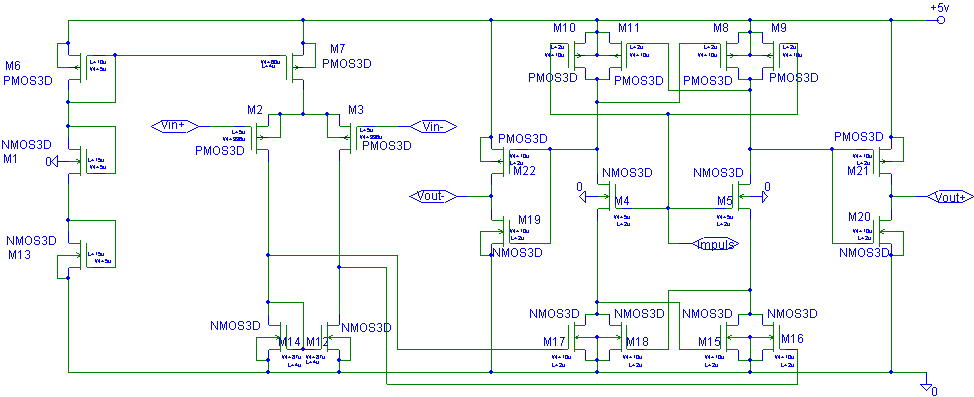
Analyzing
the literature I found that the strobed flip flop topology would bee the most promising. This
circuit employs a latched flip flop, controlled by a differential amplifier. The flip flop is clocked. Depending on
the input, the output will
fall either in one or other state.
Armed with this theory I did design the comporator in a 2mm technology (yes, 2µm, we are talking 1998). Besides the comparator core, several other circuit blocks were needed, like a catching circuit, a digital control logic, RC- oscillator, … ect. I designed the circuit around a 33 MHz clock in order to achieve the specified 30 ns.
Anyway – I did learn a lot about integrated circuit design and I used this knowledge 1:1 for my master degree.
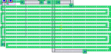
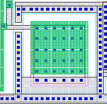
Because it looks interesting, I want to show what integrated devices look like. For doing the layout you principally have to draw a whole lot of rectangles and polygons. You have to know the different layers (vias, polysilicon, wires, …) and the minimum distances. At the end the CADence checks whether all distances are ok and the layout represents the circuit.
The layout of integrated devices look like this:
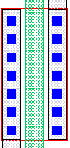
polysilicon resistor
NMOS transistor
MOS capacitor
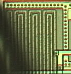
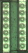
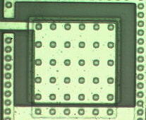
Layout of the comparator circuit above.
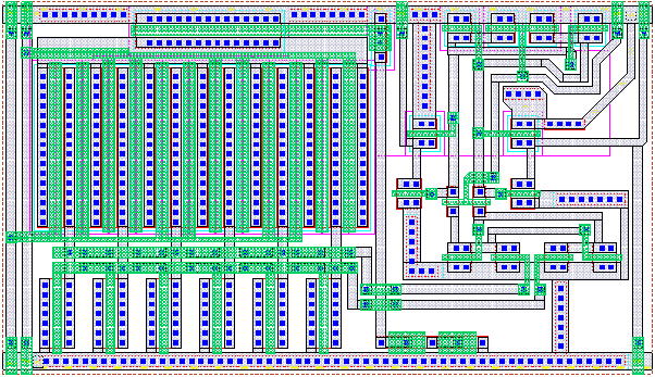
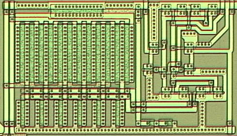
After the layout was done, a program is reads the circuit backwards from the layout. This program tries to find the electrical devices from the geometries in the layout. The result is a so called netlist, which represents the circuit of the layout. This netlist contens more devices than the original circuit because it of parasitic elements, like the capacitance of the wires. These parasites can have a big influence on the functionality of the circuit. Therefore it is important to simulate the circuit again, proving it is still working. Sometimes the circuit or layout has to be changed afterwards.
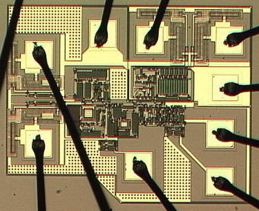
I taped out the chip at the
end of my work and it had it's fab out after I left university and was tested
then. The measurements
proofed the functionality and fulfilled the expectation. The study year work has been graded with mark 1.3
(very good).
Impressum, Disclaimer & Datenschutz
![]()